Fabrication and Characterization of Zinc Oxide Nanorods
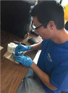
Zinc oxide (ZnO) is a wide bandgap semiconductor that has outstanding material properties. ZnO nanorods are advantageous because they can be used in various optoelectronic applications due to their extremely large surface area. The synthesis of these nanorods can be achieved through several different thin film deposition techniques. This spring semester, I worked on a project which used a process called electrochemical deposition (ECD) to create these nanorods on indium tin oxide (ITO) coated glass substrates. Such a process is cost-effective, easy to operate and scale up. After the fabrication process, I analyzed the dimensions and population density of the nanorods using a scanning electron microscope (SEM) in the Keck Microanalysis Laboratory and a UV-Vis spectrometer in the laser lab. The purpose of my research was to measure the change in the physical properties of zinc oxide nanorods caused by varying parameters, such as the molarity of the solution used, during the ECD process.
 I had several opportunities to utilize problem solving and critical thinking during my research. The first several samples I made using the ECD process were not suitable for measurements. They either broke while being mounted into the deposition cell or they cracked during the deposition due to the fragile nature of these thin glass substrates. It wasn’t until the sixth sample that I was actually able to do a deposition correctly, and the main difference here was the size of the indium wires I used as electrical contact points while mounting the sample into the cell properly. It may seem trivial, but it turns out the electrical connection component of the deposition cell was critical in creating a quality deposition. I became very familiar with operating the SEM and got a lot of experience with imaging the samples.
After graduation, I intend to gain employment at one of the local material science institutions here in Santa Rosa, whether that is in the field of thin film optics, like my research project, or in some other subcategory of that discipline.